The first speaker was Dr. Winco Yung (Asso. Professor of ISE, PolyU; Honorary Advisor, Hong Kong Printed Circuit Association – HKPCA; Center-in-charge, PCB Technology Center, PolyU) and his topic was “PCB Laminate Characterization and Quality Assurance”.

Dr. Yung presentation included PCB Lamination Technology, Common Defects in Lamination, Type of PCB Laminates, Material Characterization, Reliability Test and Case Study.

Firstly, Dr. Yung introduced the multi-layer fabrication. It begins with the selection of an inner layer core- or thin laminate material of the proper thickness. Cores could very from 0.038” to 0.005” thick and the number of cores used would be depended upon the board’s design. The basic materials of multi-layer board included copper foil, prepreg and inner-layer cores (copper foil and Glass fiber & resin).

Then the laminate panels bonded together under heat and pressure.

The typical pressing profile was shown.

The following common defects included Bow & Twist, Delamination, Blister, Measling, Misregistration, and Other defects were discussed.
I. Bow & Twist

II. Delamination

III. Blister

IV. Measling

V. Misregistration

The first five defects were summarized in the following table.

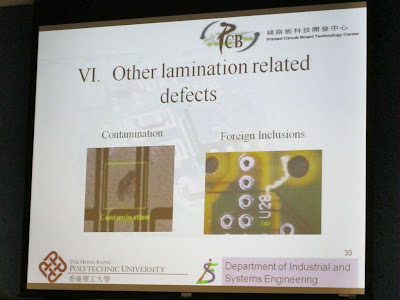
VI. Other defects

Other defects were summarized.

Then Dr. Yung briefed different type of PCB laminate such as FR4 (most economic), Halogen Free, High Speed and Flexible Materials.

After that Dr. Yung mentioned those materials characterization included:
1. Thermal properties
- Glass Transition Temperature (Tg) using TMA (Thermo-mechanical Analysis): Higher Tg, Higher Cost
- Coefficient of Thermal Expansion (CTE): Low CTE (z-axis)
- Decomposition Temperature (Td): High Td, Higher final product reliability
2. Electrical properties
- Dielectric constant (Dk) affect the signal speed
- Dissipation factor (Df) affect the signal integrity
Reliability Test for PCB (Thermal Shock, Interconnect Stress, Conductive Anodic Filament and Time to Delamination Test) was also discussed.
Conductive Anodic Filament (CAF) failure was the growth or electro-migration of copper in a PCB. The test was reference to the standard IPC-TM-650 2.6.25.
Finally, Dr. Yung discussed three case studies to us.
After the presentation, the souvenir was presented to Dr. Yung.
(Left: Dr. Raymon Chan (Specialist, MAL-HKSTP), Dr. Winco Yung and Ms.Trace Chan (Head – Membership & Promotion, HKEIA))
The second speaker was Dr. Cindy Xi (Specialist, MAL – HKSTP) and her topic was “Applications of surface analysis techniques including SEM/EDX, AES, XPS, ToF-SIMS, Surface profilometer, AFM, FTIR and XRF for PCB industry”.
Dr. Xi introduced each analysis techniques and its application in Material Analysis Laboratory (MAL) at HKSTP. Some equipment were showed in following photos.
Reference:
Hong Kong Printed Circuit Association: http://www.hkpca.org/
PCB Technology Centre: http://www.pctech.ise.polyu.edu.hk/
MAL, HKSTP:
http://lab.hkstp.org/e/default_home.asp?url=/e/customize/analysis_MAL_introduction.asp
The Hong Kong Electronic Industries Association (HKEIA):
http://www.hkeia.org/
Hong Kong Printed Circuit Association: http://www.hkpca.org/
PCB Technology Centre: http://www.pctech.ise.polyu.edu.hk/
MAL, HKSTP:
http://lab.hkstp.org/e/default_home.asp?url=/e/customize/analysis_MAL_introduction.asp
The Hong Kong Electronic Industries Association (HKEIA):
http://www.hkeia.org/


沒有留言:
發佈留言