
Prof. Ka Ming Ng (CEO, NAMI) was the first speaker who introduced NAMI background to us. NAMI has established since 2006 and it was a not-for-profit company incorporated by ITC and hosted by HKUST. The role of NAMI is undertaken and provided funding for industry-oriented research in nanotechology and advanced materials, as well as, offer market-driven innovative solutions to local industries by transforming scientific advancements into marketable products.

Prof. Ng said NAMI worked as Technology Marketplace through the steps: What-to-make -> How-to-mark -> Material -> Process. NAMI's approach and strategy was as bridge for both investors and innovators through networking, expertise and funding. NAMI separated into five clusters included Sustainable Energy, Solid State Lighting and Display, Environmental Technologies, Construction/Building Materials, and Bio & Healthcare Products. At the end, Prof. Ng said NAMI planned to relocate their Headquarters from HKUST to Hong Kong Science Park.

The second speaker was Dr. Peter W. Lee (CTO, NAMI) and he introduced NAMI's five clusters technologies.

For PhotoVolitaic (PV) Technology , Thin Film CIGS manufacturing process development and Organic PV (OPV) materials were under development. Other technologies were briefed including Printable Conductor from Nanoparticle Ink, Printed Si NPs Thermistor Array, Printed Temperature Sensors, Printable Low Cost OLED Display, Doped Nano Lithium Titanate (LTO), LED Thermal Management, Multifunctional Environmental Friendly Paint, etc.

After the talk, we took a group photo.

Then we visited different laboratories in HKUST. The first place was Materials Characterization and Preparation Facility (MCPF).

X-ray diffraction spectrometer

Transmission Electron Microscopy (TEM)

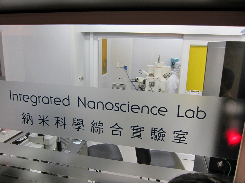
Then we visited Integrated Nano science Lab.
The clean room installed yellow lamp in which UV was removed. The area of photo was buffer area that no mask operation.

General area for R&D of wafer process

The lab representative explained the making of an Integrated Circuit from mask design and layout to wafer produced.

Reference:
HKCCMA - http://www.hkccma.org/
HKPC - http://www.hkpc.org/
HKETA - http://www.hketa.org.hk/
HKSQ - http://www.hksq.org/
NAMI - https://www.nami.org.hk/

沒有留言:
發佈留言