顯示包含「Solar Tech Training」標籤的文章。顯示所有文章

2010年10月15日星期五

Spectroscopic Ellipsometer for Solar Thin Film Analysis

I would like to share the training of Ellipsometer for Solar Thin Film analysis on 13th to 14th October 2010 in Hong Kong Science and Technology Park (HKSTP).


The trainer was Mr. Charles Lin (Application Engineer, Radiation Technology Co., Ltd.) and his training topic entitled “Spectroscopic Ellipsometers and their extension by SOPRA” and the training included theoretical and practical session.


Firstly, Mr. Lin introduced the instrumentation of Ellipsometer. The detector range of the Ellipsometer which employed in HKSTP was from 170nm to 2000nm (From deep UV to NIR). Mr. Lin also briefed some optional sources below:
· GXR Option (X-ray Reflectometry) – Lithography, advanced semiconductor films (high absorption – k)
· IRSE Option – dielectric films & materials characterization doped semiconductors epi layers
· EPA Option – fundamental research on porous thin films
· Cryostat Option – fundamental research superconductive materials


Then the optical schema was showed. Xe Lamp was used as source and installed shutter to reduce the background signal. The attenuators in front of Xe Lamp used to reduce the intensity. The diaphragm worked like Iris. The microspot was employed which is 200μm (diameter) for focus (a series of lens). After reflected on the sample surface, the signal received from detector. The optional compensator was specific for small absorption (k) but it was not installed in HKSTP’s ellipsometer.


The following diagrams showed the overlapping of parallel beams from back side reflection. That was why microspots should be used to avoid the overlapping effect. (The substrate thickness of sample should be larger than 0.7mm.)


Then he mentioned different analysis methodology. However, we need to understand the sample characteristic such as approximate thickness, reflective index (n) and absorption (k) before analysis.


The Bulk substrate model was used for non-transparent material or metal substrate.


Dispersion law was commonly used in the analysis but it was found difficult to analyze too thick sample.


Lastly, he concluded the precise and reproducible optical set up plus advanced modeling software could come out the good result of analysis.


The practical part was demonstrated the operation of Ellipsometer. The trainer set up the ellipsometer.


He showed us the sample which was Silicon Nitride (Si3N4).


The properties of SiO2 and Si3N4 were showed in the Table 1.


Then engineer turned the distance of stage to optimize the signal.


Close shot of Si3N4 sample


Find the maximum intensity when turn the equipment.


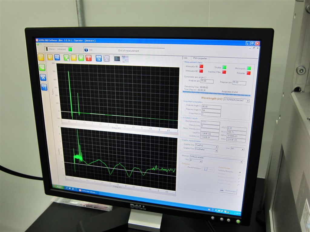
The lower diagram of the following photo showed three peaks and each peak represented about 1000Å thickness.

Engineer prepared the other sample which was SiO2.


Close shot of SiO2 sample


The lower diagram of the following photo showed many peaks indicating that SiO2 sample was much thicker than Si3N4 sample.


And then using modeling simulation calculated the actual thickness of that sample.


I took a photo with the Ellipsometer.


For more information:
PV Testing Laboratory Service in HKSTP: http://lab.hkstp.org/e/default_home.asp?url=/e/customize/analysis_solar.asp
Radiation Technology Co., Ltd.: www.raditech.com.tw

2010年8月27日星期五

Workshop on Raman Spectroscopy for Photovoltaic Application

A training workshop entitled “Usage of Raman Spectroscopy” was organized by Hong Kong Science & Technology Parks (HKSTP) on 27 August 2010. The Photovoltaic (PV) Test Laboratory in HKSTP is equipped with a series of analytical instruments for the analysis of photovoltaic devices. Raman spectroscopy is one of instrument to provide a wide range of applications in PV product.

Mr. Edward Chen (Manager, Technical Support & Marketing Group, AST Instruments Corporation) was a speaker, who introduced the Raman Spectroscopy and its application.


In the beginning, he briefed the history of Raman which was discovered by Dr. C.V. Raman form India in 1928.


In the beginning, he briefed the history of Raman which was discovered by Dr. C.V. Raman form India in 1928.


The principle of Raman was introduced.
Raman spectra are obtained by irradiating a sample with a powerful source of visible monochromatic radiation (e.g. Argon Laser – 488nm (20492cm-1). The scattered radiation, which was observed at 90 degree to the incident beam, is of three types. They are Stokes, Anti-Stokes and Rayleigh.


The advantage and characteristic of Raman included:
i) Fingerprint for qualitative identification
ii) No sample preparation
iii) Fast and non destructive, and
iv) Highly selective technique.

The following photo showed the instrumentation of Raman Spectroscopy System.


The common lasers used in Raman are Ar, He-Ne and He-Cd.
The following range usually employed:
UV Range: 244, 257, 266, 325, 355, 364nm
VIS Range: 488, 514, 532, 633nm
NIR Range: 785, 830nm


The advantage and disadvantage of working at different wavelengths were shown below.


Raman is a very powerful technique to characterize organic or inorganic compounds. There are many fields of application included Semiconductors, Polymers, Geology/Mineralogy/Gemology, Carbon Compounds, Life Science, Forensics, Pharmaceuticals, Chemistry, Environmental, Physics, Art & Culture, Thin Films, etc.


Then Mr. Edward Chen focused on Photovoltaic applications. There are three main types of photovoltaic (PV) materials included:
· Silicon – the most popular
· Compounds with Cu, In, Ga, S, Se, Cd
· Organic


For silicon based photovoltaic, the following characteristics were stated.
· Crystalline silicon (c-Si) is the most efficient, but very expensive to produce due to the high energy consumption for purification and crystallization.
· Amorphous Silicon (a-Si) is less expensive but less efficient.
· Polycrystalline Silicon (p-Si): Solutions are investigating.

The Raman spectra of these three silicon phases were showed.

The measurement of the ratio between c-Si and a-Si is the main application of Raman spectroscopy.

The following photo demonstrated the stress analysis on silicon material.


Different wavelength had different depth penetration in crystalline silicon.


Mr. Chen introduced different compounds based solar materials such as CIGS (CuInGaSe), CuInSe, CdS, etc.

Finally, Mr. Chen concluded:
i) A variety of silicon samples have been analysed exhibiting different extremes of amorphous and crystalline structure.
ii) Mapping method was used to gain high quality Raman data much faster then point analysis methods. This is due to the reduced laser power density, but increase in the amount of sample being analyzed.

LinkWithin

Related Posts with Thumbnails