Firstly, Professor Kam-Sing WONG (President, Physical Society of Hong Kong) presented welcome message to us.

The first speaker was Mr. Daniel CHAN (Global PCB Council Chairman, IBM Hong Kong Limited). His topic for keynote speech was “PCB and Packaging Industry Trend-Opportunity and Challenge in 2009”.
Mr. Chan introduced the global economic outlook that 2009 is a year of challenge and global economy would be gradual recovery in 2010 and beyond. Then he pointed out some opportunities in Pearl River Delta at GuangDong:
- Transformed to a modern intelligent based 1 billion population economic system
- Knowledge based society particularly Hong Kong
- Highly competitive in globalization process

Corporate Social Responsibility (CSR) value curve has became more important. PCB and Electronics Industry’s “3D” Approach was shown:
i) DEEPER Client Relationships
ii) DIFFERENTIATED Solutions
iii) Global DELIVERY
Finally, he summarized the topic by using the sentence “The Electronics Industry is looking for your expertise in building innovative, end-to-end, competitive, sustainable, and high quality solutions. Your success is critical for creating greater value for both tangible and intangible business results in the Industry.”
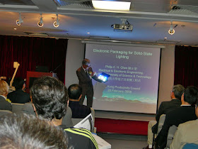 He showed the development history of white LED and its application to us.

Then he explained their MTR project which had started since 2006. During Q&A, one of participant asked why the LED light of MTR was observed grid shape. Prof. CHAN explained that if a filter is added to make it smoother, passengers will not know we are using LED. (Interesting!)

After that he introduced the LED manufacturing process and some electronic packaging issues such as Thermal management, Epoxy and silicon encapsulation, Integration of phosphor, Integration of optics and Integration of lighting system.
Dr. Ivan SHAM (Manager, ASTRI) was the third speaker and his presentation entitled “Flip Chip and Wafer-Level Chip Scale Packaging: Market Updates, Key Processes and Application Examples”. He introduced Flip Chip (FC) packaging market and key processes. Wafer-Level Chip-Scale Packaging (WL-CSP) was also discussed.

What is WL-CSP?
· Semiconductor packaging in which the majority of the packaging and testing is accomplished in whole-wafer form.
· The device must have:
- Redistribution layer (RDL) for electrical redistribution
- Interconnect between chip and board
- Environmental/mechanical protection
Finally, speaker summarized that the futures of FC would be primarily related to high pin counts, high performance applications while WL-CSP would be more suitable for low pin counts, low-cost applications.
- Transformed to a modern intelligent based 1 billion population economic system
- Knowledge based society particularly Hong Kong
- Highly competitive in globalization process

Corporate Social Responsibility (CSR) value curve has became more important. PCB and Electronics Industry’s “3D” Approach was shown:
i) DEEPER Client Relationships
ii) DIFFERENTIATED Solutions
iii) Global DELIVERY
Finally, he summarized the topic by using the sentence “The Electronics Industry is looking for your expertise in building innovative, end-to-end, competitive, sustainable, and high quality solutions. Your success is critical for creating greater value for both tangible and intangible business results in the Industry.”
The second speaker was Prof. Philip CHAN (Dean of Engineer, Director of Center for Advanced Microsystems Packaging, HKUST) and topic presented “Electronic Packaging for Solid-State Lighting”. Before starting the presentation, Prof. CHAN demonstrated the LED panel which was 60 Lumen/Watt and 2006 technology. (Because the LED lighting was very bright, Prof. CHAN needed to wear protective goggle.)
 He showed the development history of white LED and its application to us.
Then he explained their MTR project which had started since 2006. During Q&A, one of participant asked why the LED light of MTR was observed grid shape. Prof. CHAN explained that if a filter is added to make it smoother, passengers will not know we are using LED. (Interesting!)

After that he introduced the LED manufacturing process and some electronic packaging issues such as Thermal management, Epoxy and silicon encapsulation, Integration of phosphor, Integration of optics and Integration of lighting system.
Dr. Ivan SHAM (Manager, ASTRI) was the third speaker and his presentation entitled “Flip Chip and Wafer-Level Chip Scale Packaging: Market Updates, Key Processes and Application Examples”. He introduced Flip Chip (FC) packaging market and key processes. Wafer-Level Chip-Scale Packaging (WL-CSP) was also discussed.

What is WL-CSP?
· Semiconductor packaging in which the majority of the packaging and testing is accomplished in whole-wafer form.
· The device must have:
- Redistribution layer (RDL) for electrical redistribution
- Interconnect between chip and board
- Environmental/mechanical protection
Finally, speaker summarized that the futures of FC would be primarily related to high pin counts, high performance applications while WL-CSP would be more suitable for low pin counts, low-cost applications.
The 4th speaker was Dr. Daniel SHI (Director, ASTRI) and his topic entitled “3D Intergration – A Solution for Next Generation Silicon Devices”.

He explained the 3D packaging was heterogeneous integrated such as RF, memory, logic, MEMS, imagers, etc. Through Silicon Via (TSV) Based 3D packaging was shown.

Lastly, he summarized the 3D integration was another major solution to increase IC density and functionality and 3D packaging/integration technology was believed to have many applications including consumer electronics, wireless communication, bio-medical devices, aerospace, automotive, etc.
Mr. Tetsuya OHISHI (Consultant, Grand Joint Technology Ltd.) was the 5th speaker and presented “Embedded Component Trend & Applications”. He introduced companies and technology about embedded process / assembly in Japan.

He introduced some project in Hong Kong.

He introduced the related conference in Japan.

Mr. Jun WU (Sr. Application Engineer, Cadence Design System, Inc.) was the 6th speaker and his topic was “Advanced IC Package/SiP and PCB Co-Design solution”. He took the design challenges:
- High-level system integration on silicon driving pin count over 1000 pins
- High speed digital I/O’s
- Minimizing package cost

Then Mr. WU introduced Package and PCB co-design with SCM.

Then Mr. WU introduced Package and PCB co-design with SCM.
“Flow by Functions” was introduced:
i) System Conectivity
ii) VSIC Model
iii) IO Floorplan
iv) SiP Substrate Floor Plan
v) Electrical Verification
vi) Substrate Routing

At the end, he demonstrated the Storyboard.

The 7th speaker was Prof. Winco YUNG (Asso Prof, ISE Dept., PolyU) and his presentation entitled “Green PCB and Substrate for Sustainability”.

Firstly, he introduced environmental policy in Europe (e.g. REACH timeline) and in China.

Then he discussed environmental research for Green PCB Material as follows:
i) Elimination of Halogenated Flame Retardants
ii) Reduction of Toxic Solvents
iii) Renewable Resin for PCBs
Finally, he concluded:
i) It is inevitable that the transition to environmental compliance will have a significant impact on the business landscape in PCB and electronic industries.
ii) Capability & Timeliness to comply with RoHS, WEEE, REACH and China environmental regulations now become key competitive differentiators in the industry.
The 8th speaker was Miss Tarja RAPALA (CTO, Meadville Group) and her topic was “HDI PCBs application of Mobile devices: Trends and opportunities”.

She introduced mobile device and technology development. Then she discussed the driver for PCB technologies in mobile devices including:
- Product segment and type (Low-, mid-, high end device)
- Component packaging technologies

Finally, she reviewed that component I/O count increase and continuous pressure on miniaturization are driving PCB technology selection in mid-/high-end mobile devices; but in low-end products were driven by cost and availability.
Mr. Daniel CHAN (Global PCB Council Chairman, IBM Hong Kong Limited) gave the 9th speech and presented “Global Computer Server Infra-Structure – PCB Challenge and Opportunity in 2009”.

He presented PCB technology trend for processing power demanding server as follows:
- Higher layer count
- Larger form factor
- Signal integrity challenge
- Environmental sustainability
- High reliability requirement

Then he showed different series product which are made by using optical fiber.


Lastly, he gave the key message “The server supply market is looking for overall competitive end to end PCB solutions in both commercial and technical perspective to create an unmatchable value in both tangible and intangible perspective to our client business success.”
Dr. Lifu YOU (China Technical Marketing Manager, System Design Division, Mentor Graphics) was the 10th speaker who presented “PCB Design Collaboration – Enabling Design with Distributed, Multi-disciplined Teams”.

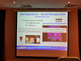
He introduced “XtremePCB” design tools which were able to provide multi-designer simultaneous layout. One of their client commented the use of XtremePCB reduced the design cycle time from 13 weeks to 5 weeks.
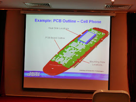
He used cell phone as one of examples.
The 11th speaker was Mr. P.C. LEUNG (Director, Year 2000 Ltd) and his topic was “Welding Technology Used in Repair”.
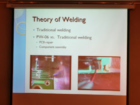
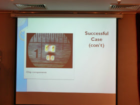
He also showed several success cases including super mini motor, mobile phone speaker, chip components (~2mm size), PCBA repair (0.3mm pitch), etc.
He concluded that engineering / R&D departments could adopt welding machine as an essential tool, along side power supplies, soldering irons, and screwdrivers.
By the end of seminar, Mr. Raymond CHIU (Principal Consultant, Automotive and Electronics Division, HKPC) introduced PCB laboratories in HKPC and led plant tour for HKPC reliability and EMC laboratories.

He explained the 3D packaging was heterogeneous integrated such as RF, memory, logic, MEMS, imagers, etc. Through Silicon Via (TSV) Based 3D packaging was shown.

Lastly, he summarized the 3D integration was another major solution to increase IC density and functionality and 3D packaging/integration technology was believed to have many applications including consumer electronics, wireless communication, bio-medical devices, aerospace, automotive, etc.
Mr. Tetsuya OHISHI (Consultant, Grand Joint Technology Ltd.) was the 5th speaker and presented “Embedded Component Trend & Applications”. He introduced companies and technology about embedded process / assembly in Japan.

He introduced some project in Hong Kong.

He introduced the related conference in Japan.

Mr. Jun WU (Sr. Application Engineer, Cadence Design System, Inc.) was the 6th speaker and his topic was “Advanced IC Package/SiP and PCB Co-Design solution”. He took the design challenges:
- High-level system integration on silicon driving pin count over 1000 pins
- High speed digital I/O’s
- Minimizing package cost

Then Mr. WU introduced Package and PCB co-design with SCM.

Then Mr. WU introduced Package and PCB co-design with SCM.
“Flow by Functions” was introduced:
i) System Conectivity
ii) VSIC Model
iii) IO Floorplan
iv) SiP Substrate Floor Plan
v) Electrical Verification
vi) Substrate Routing

At the end, he demonstrated the Storyboard.

The 7th speaker was Prof. Winco YUNG (Asso Prof, ISE Dept., PolyU) and his presentation entitled “Green PCB and Substrate for Sustainability”.

Firstly, he introduced environmental policy in Europe (e.g. REACH timeline) and in China.

Then he discussed environmental research for Green PCB Material as follows:
i) Elimination of Halogenated Flame Retardants
ii) Reduction of Toxic Solvents
iii) Renewable Resin for PCBs
Finally, he concluded:
i) It is inevitable that the transition to environmental compliance will have a significant impact on the business landscape in PCB and electronic industries.
ii) Capability & Timeliness to comply with RoHS, WEEE, REACH and China environmental regulations now become key competitive differentiators in the industry.
The 8th speaker was Miss Tarja RAPALA (CTO, Meadville Group) and her topic was “HDI PCBs application of Mobile devices: Trends and opportunities”.

She introduced mobile device and technology development. Then she discussed the driver for PCB technologies in mobile devices including:
- Product segment and type (Low-, mid-, high end device)
- Component packaging technologies

Finally, she reviewed that component I/O count increase and continuous pressure on miniaturization are driving PCB technology selection in mid-/high-end mobile devices; but in low-end products were driven by cost and availability.
Mr. Daniel CHAN (Global PCB Council Chairman, IBM Hong Kong Limited) gave the 9th speech and presented “Global Computer Server Infra-Structure – PCB Challenge and Opportunity in 2009”.

He presented PCB technology trend for processing power demanding server as follows:
- Higher layer count
- Larger form factor
- Signal integrity challenge
- Environmental sustainability
- High reliability requirement

Then he showed different series product which are made by using optical fiber.


Lastly, he gave the key message “The server supply market is looking for overall competitive end to end PCB solutions in both commercial and technical perspective to create an unmatchable value in both tangible and intangible perspective to our client business success.”
Dr. Lifu YOU (China Technical Marketing Manager, System Design Division, Mentor Graphics) was the 10th speaker who presented “PCB Design Collaboration – Enabling Design with Distributed, Multi-disciplined Teams”.

He introduced “XtremePCB” design tools which were able to provide multi-designer simultaneous layout. One of their client commented the use of XtremePCB reduced the design cycle time from 13 weeks to 5 weeks.

He used cell phone as one of examples.

The 11th speaker was Mr. P.C. LEUNG (Director, Year 2000 Ltd) and his topic was “Welding Technology Used in Repair”.

He also showed several success cases including super mini motor, mobile phone speaker, chip components (~2mm size), PCBA repair (0.3mm pitch), etc.

He concluded that engineering / R&D departments could adopt welding machine as an essential tool, along side power supplies, soldering irons, and screwdrivers.
By the end of seminar, Mr. Raymond CHIU (Principal Consultant, Automotive and Electronics Division, HKPC) introduced PCB laboratories in HKPC and led plant tour for HKPC reliability and EMC laboratories.


不錯的blog,加油!
回覆刪除Oggie
Doggie